- 您现在的位置:买卖IC网 > Sheet目录1998 > ICS843251AG-04LF (IDT, Integrated Device Technology Inc)IC CLK GENERATOR LVPECL 8-TSSOP
ICS843251-04
FEMTOCLOCKCRYSTAL-TO-3.3V LVPECL CLOCK GENERATOR
IDT / ICS 3.3V LVPECL CLOCK GENERATOR
3
ICS843S51AG-04 REV. A JANUARY 12, 2009
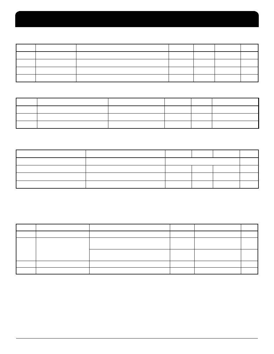
Table 3B. LVCMOS/LVTTL DC Characteristics, VCC = 3.3V ± 5%, VEE = 0V, TA = 0°C to 70°C
Table 3C. LVPECL DC Characteristics, VCC = 3.3V ± 5%, VEE = 0V, TA = 0°C to 70°C
NOTE 1: Outputs termination with 50
to V
CC – 2V.
Table 4. Crystal Characteristics
AC Electrical Characteristics
Table 5. AC Characteristics, VCC = 3.3V ± 5%, VEE = 0V, TA = 0°C to 70°C
NOTE: Electrical parameters are guaranteed over the specified ambient operating temperature range, which is established when the
device is mounted in a test socket with maintained transverse airflow greater than 500 lfpm. The device will meet specifications after
thermal equilibrium has been reached under these conditions.
NOTE 1: Please refer to Phase Noise Plots.
Symbol
Parameter
Test Conditions
Minimum
Typical
Maximum
Units
VIH
Input High Voltage
2
VCC + 0.3
V
VIL
Input Low Voltage
-0.3
0.8
V
IIH
Input High Current
VCC = VIN = 3.465V
150
A
IIL
Input Low Current
VCC = 3.465V, VIN = 0V
-5
A
Symbol
Parameter
Test Conditions
Minimum
Typical
Maximum
Units
VOH
Output High Current; NOTE 1
VCC – 1.4
VCC – 0.9
A
VOL
Output Low Current; NOTE 1
VCC – 2.0
VCC – 1.7
A
VSWING
Peak-to-Peak Output Voltage Swing
0.6
1.0
V
Parameter
Test Conditions
Minimum
Typical
Maximum
Units
Mode of Oscillation
Fundamental
Frequency
19.33
30
MHz
Equivalent Series Resistance (ESR)
50
Shunt Capacitance
7pF
Symbol
Parameter
Test Conditions
Minimum
Typical
Maximum
Units
fOUT
Output Frequency
145
187.5
MHz
tjit()
RMS Phase Jitter, Random;
NOTE 1
156.25MHz,
(Integration Range: 1.875MHz – 20MHz)
0.39
ps
187.5MHz,
(Integration Range: 1.875MHz – 20MHz)
0.40
ps
tR / tF
Output Rise/Fall Time
20% to 80%
285
415
ps
odc
Output Duty Cycle
48
52
%
发布紧急采购,3分钟左右您将得到回复。
相关PDF资料
ICS843251AGI-14LF
IC CLK GEN ETHERNET 25MHZ 8TSSOP
ICS843251BGI-12LF
IC CLK GENERATOR LVPECL 8-TSSOP
ICS843251BGI-15LF
IC CLK GEN ETHERNET 25MHZ 8TSSOP
ICS843253AGI-45LF
IC SYNTHESIZER LVPECL 16-TSSOP
ICS8432DY-101LFT
IC SYNTHESIZER 700MHZ 32-LQFP
ICS8432DYI-101LF
IC SYNTHESIZER 700MHZ 32-LQFP
ICS843SDNAGLF
IC GENERATOR FEMTOCLOCK 8TSSOP
ICS844001AGLFT
IC CLK GEN FIBRE CHAN 8-TSSOP
相关代理商/技术参数
ICS843251AG-04LFT
功能描述:IC CLK GENERATOR LVPECL 8-TSSOP RoHS:是 类别:集成电路 (IC) >> 时钟/计时 - 时钟发生器,PLL,频率合成器 系列:HiPerClockS™, FemtoClock™ 标准包装:1,000 系列:- 类型:时钟/频率合成器,扇出分配 PLL:- 输入:- 输出:- 电路数:- 比率 - 输入:输出:- 差分 - 输入:输出:- 频率 - 最大:- 除法器/乘法器:- 电源电压:- 工作温度:- 安装类型:表面贴装 封装/外壳:56-VFQFN 裸露焊盘 供应商设备封装:56-VFQFP-EP(8x8) 包装:带卷 (TR) 其它名称:844S012AKI-01LFT
ICS843251AG-04T
制造商:ICS 制造商全称:ICS 功能描述:FEMTOCLOCKS⑩ CRYSTAL-TO-3.3V LVPECL CLOCK GENERATOR
ICS843251AGI-04LF
功能描述:IC CLK GENERATOR LVPECL 8-TSSOP RoHS:是 类别:集成电路 (IC) >> 时钟/计时 - 时钟发生器,PLL,频率合成器 系列:HiPerClockS™, FemtoClock™ 标准包装:27 系列:Precision Edge® 类型:频率合成器 PLL:是 输入:PECL,晶体 输出:PECL 电路数:1 比率 - 输入:输出:1:1 差分 - 输入:输出:无/是 频率 - 最大:800MHz 除法器/乘法器:是/无 电源电压:3.135 V ~ 5.25 V 工作温度:0°C ~ 85°C 安装类型:表面贴装 封装/外壳:28-SOIC(0.295",7.50mm 宽) 供应商设备封装:28-SOIC 包装:管件
ICS843251AGI-04LFT
功能描述:IC CLK GENERATOR LVPECL 8-TSSOP RoHS:是 类别:集成电路 (IC) >> 时钟/计时 - 时钟发生器,PLL,频率合成器 系列:HiPerClockS™, FemtoClock™ 标准包装:27 系列:Precision Edge® 类型:频率合成器 PLL:是 输入:PECL,晶体 输出:PECL 电路数:1 比率 - 输入:输出:1:1 差分 - 输入:输出:无/是 频率 - 最大:800MHz 除法器/乘法器:是/无 电源电压:3.135 V ~ 5.25 V 工作温度:0°C ~ 85°C 安装类型:表面贴装 封装/外壳:28-SOIC(0.295",7.50mm 宽) 供应商设备封装:28-SOIC 包装:管件
ICS843251AGI-14LF
功能描述:IC CLK GEN ETHERNET 25MHZ 8TSSOP RoHS:是 类别:集成电路 (IC) >> 时钟/计时 - 时钟发生器,PLL,频率合成器 系列:HiPerClockS™, FemtoClock™ 标准包装:27 系列:Precision Edge® 类型:频率合成器 PLL:是 输入:PECL,晶体 输出:PECL 电路数:1 比率 - 输入:输出:1:1 差分 - 输入:输出:无/是 频率 - 最大:800MHz 除法器/乘法器:是/无 电源电压:3.135 V ~ 5.25 V 工作温度:0°C ~ 85°C 安装类型:表面贴装 封装/外壳:28-SOIC(0.295",7.50mm 宽) 供应商设备封装:28-SOIC 包装:管件
ICS843251AGI-14LFT
功能描述:IC CLK GEN ETHERNET 25MHZ 8TSSOP RoHS:是 类别:集成电路 (IC) >> 时钟/计时 - 时钟发生器,PLL,频率合成器 系列:HiPerClockS™, FemtoClock™ 标准包装:1,000 系列:- 类型:时钟/频率合成器,扇出分配 PLL:- 输入:- 输出:- 电路数:- 比率 - 输入:输出:- 差分 - 输入:输出:- 频率 - 最大:- 除法器/乘法器:- 电源电压:- 工作温度:- 安装类型:表面贴装 封装/外壳:56-VFQFN 裸露焊盘 供应商设备封装:56-VFQFP-EP(8x8) 包装:带卷 (TR) 其它名称:844S012AKI-01LFT
ICS843251BGI-12
制造商:ICS 制造商全称:ICS 功能描述:FEMTOCLOCKS⑩ CRYSTAL-TO-3.3V, 2.5V LVPECL CLOCK GENERATOR
ICS843251BGI-12FT
制造商:ICS 制造商全称:ICS 功能描述:FEMTOCLOCKS⑩ CRYSTAL-TO-3.3V, 2.5V LVPECL CLOCK GENERATOR